IBM 0.7nm NanoStack: Deep Dive into the Sub-1nm Semiconductor Breakthrough
Executive Summary: On June 25, 2026, IBM unveiled the world’s first sub-1nm chip technology, based on the revolutionary NanoStack 3D transistor architecture. Pushing the process node to 0.7nm (7 angstroms), the technology integrates nearly 100 billion transistors on a fingernail-sized chip, delivering up to 50% higher performance or 70% better energy efficiency compared to 2nm. This milestone marks the semiconductor industry’s transition from the “nanometer era” to the “angstrom era.” This article provides a deep technical analysis of the NanoStack architecture, its physical principles, and its profound implications for AI computing infrastructure.
I. Industry Background: Twilight of Moore’s Law and a New Dawn
1.1 The Semiconductor Physical Limit Dilemma
For the past decade, the semiconductor industry has faced a fundamental challenge: as transistor channel dimensions approach 1nm, quantum tunneling effects cause electrons to penetrate the gate insulator directly, causing standby power to skyrocket. Simultaneously, the cost of simply shrinking dimensions has grown exponentially—a single 2nm fab now costs over $30 billion, with initial yields below 55%.
Industry consensus once held that 2nm was the physical ceiling for silicon-based planar transistors. The roadmaps of Intel, TSMC, and Samsung all pointed to 1.4nm (14 angstroms) as their 2028 target, after which they entered a “dead end.” Against this backdrop, IBM’s June 25, 2026 announcement of a 0.7nm (7 angstrom) chip technology represents a leap across multiple generations, directly breaking through the previously assumed physical limit.
1.2 IBM’s “Hidden Chip Giant” Status
To understand this breakthrough, one must first understand IBM’s unique historical position in semiconductors. IBM has no fabs of its own, but it possesses the deepest fundamental R&D track record in the field:
| Year | IBM Chip Technology Milestone | Industry Impact |
|---|---|---|
| 1966 | Invention of single-transistor DRAM | Foundation of all modern memory |
| 1960s | Flip-chip packaging | Still a mainstream packaging solution |
| 1997 | Copper interconnect | Replaced aluminum, still industry standard |
| 2001 | Strained silicon | Adopted industry-wide |
| 2007 | High-k metal gate | Solved sub-45nm gate leakage |
| 2017 | Nanosheet GAA (Gate-All-Around) | Current 2nm/3nm standard |
| 2026 | NanoStack 3D stacking | Opens the angstrom era |
From copper interconnects and strained silicon to high-k metal gates and nanosheet GAA, every technology IBM pioneered became industry standards. NanoStack continues this tradition—this is not a “theoretical exercise” from a lab. IBM published complete device measurement data at VLSI 2026, completed full CMOS process bonding, and demonstrated a fully functional angstrom-scale process with complete logic and memory cell capabilities.
II. NanoStack 3D Architecture: A Deep Technical Analysis
2.1 From Planar to 3D: A Paradigm Shift
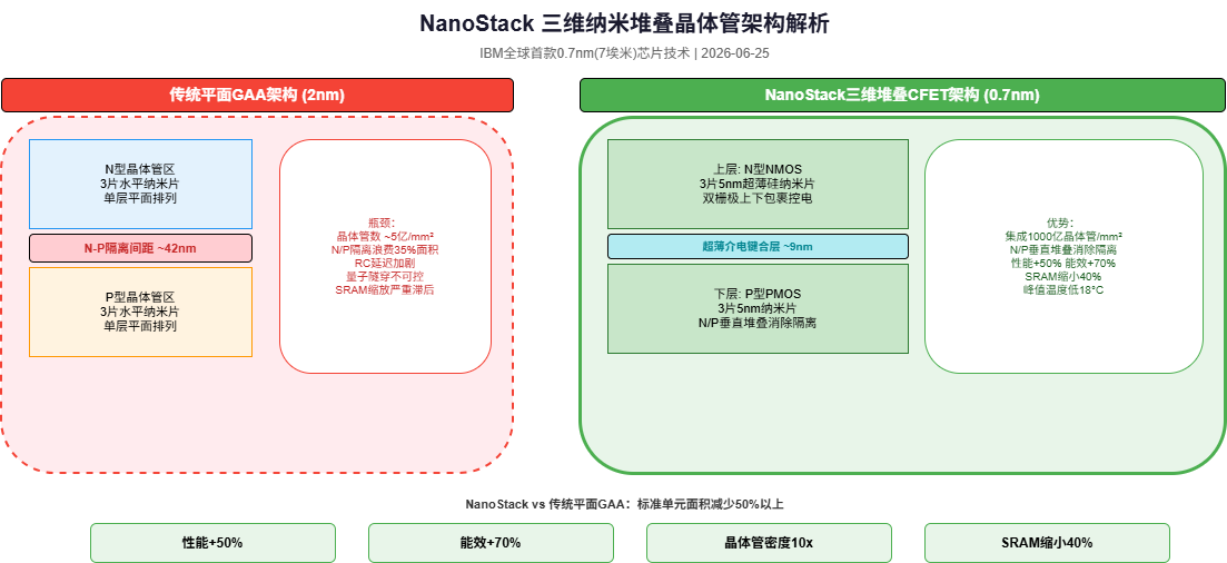
Traditional chips arrange transistors side by side on a 2D plane—the fundamental logic of Moore’s Law for over 50 years: increase density by continuously shrinking transistor spacing. But as dimensions enter the nanometer scale, this path faces three physical constraints:
- RC signal delay: Thinner metal wires have higher resistance, causing super-linear signal propagation delays
- Electromigration: High current density causes atomic migration in wires, leading to open circuits
- Quantum tunneling: When gate insulators are atomically thin, electrons pass through directly
NanoStack’s core insight: don’t make it smaller, make it taller. Instead of compressing planar spacing, it vertically stacks transistors, claiming space in the third dimension.
2.2 NanoStack Physical Architecture
import numpy as np

def analyze_nanostack_density():
    """
    Density comparison: NanoStack 3D vs traditional planar architecture

    NanoStack key parameters:
    - Dual-layer vertically bonded CFET structure
    - Upper layer NMOS, lower layer PMOS
    - 3 ultra-thin silicon nanosheets per layer, ~5nm thickness each
    - 9nm inter-layer dielectric spacing
    - Standard cell height reduced 52% vs 2nm planar
    """

    planar = {
        'node': '2nm Planar GAA',
        'cell_width_nm': 48,
        'cell_height_nm': 120,   # includes 42nm N-P isolation
        'layers': 1,
        'transistors_per_cell': 2,
    }

    nanostack = {
        'node': '0.7nm NanoStack CFET',
        'cell_width_nm': 36,     # 25% width reduction
        'cell_height_nm': 56,    # no isolation spacing needed
        'layers': 2,             # vertical stacking
        'transistors_per_cell': 2,
    }

    def calc_density(p):
        area = p['cell_width_nm'] * p['cell_height_nm']
        cells_per_mm2 = 1e12 / area
        return int(cells_per_mm2 * p['transistors_per_cell'] * p['layers'])

    d_p = calc_density(planar)
    d_n = calc_density(nanostack)

    print("=" * 65)
    print("NanoStack vs Planar GAA Density Comparison")
    print("=" * 65)
    print(f"\n{'Parameter':<28} {'2nm GAA':<18} {'0.7nm NanoStack':<18}")
    print("-" * 60)
    print(f"{'Cell Width (nm)':<28} {planar['cell_width_nm']:<18} {nanostack['cell_width_nm']:<18}")
    print(f"{'Cell Height (nm)':<28} {planar['cell_height_nm']:<18} {nanostack['cell_height_nm']:<18}")
    print(f"{'Effective Area (nm²)':<28} {planar['cell_width_nm']*planar['cell_height_nm']:<18} {nanostack['cell_width_nm']*nanostack['cell_height_nm']:<18}")
    print(f"{'Vertical Layers':<28} {planar['layers']:<18} {nanostack['layers']:<18}")
    print(f"{'Transistors/mm²':<28} {d_p:<18,} {d_n:<18,}")
    print(f"\nNanoStack Density Gain: {d_n/d_p:.2f}x")

    # IBM verified data
    ibm_2nm = 500_000_000
    ibm_07nm = 986_000_000
    print(f"\nIBM Measured Data:")
    print(f"  2nm Nanosheet: {ibm_2nm:,} transistors/mm²")
    print(f"  0.7nm NanoStack: {ibm_07nm:,} transistors/mm²")
    print(f"  IBM verified gain: {ibm_07nm/ibm_2nm:.2f}x")
    print(f"  1cm² chip integrates: {ibm_07nm * 100:,} transistors")
    print(f"  (Approaching 100 billion on fingernail-sized die)")

analyze_nanostack_density()
2.3 Key Technical Innovations
1. 3D Sequential Integration
The most fundamental innovation in NanoStack is not shrinking transistors but stacking them vertically. Each standard cell consists of two complete transistor layers bonded through an ultra-thin dielectric layer: NMOS on top, PMOS below. This design directly eliminates the isolation spacing required between N and P transistors in planar designs—at 2nm, this gap was approximately 42nm, consuming 35% of the standard cell height.
2. Dual-Channel Independent Optimization
Because the two layers are fabricated separately on different wafers before bonding, each layer can use different material compositions. Engineers can independently select optimal channel materials for NMOS and PMOS transistors, optimizing performance and power separately. This is impossible in planar architectures where N and P transistors must share the same fabrication process.
3. Ruthenium Interconnects
NanoStack’s interconnect layers replace traditional copper with ruthenium. At angstrom-scale wire dimensions, copper electromigration becomes severe—copper atoms migrate under electron flow, eventually causing open circuits. Ruthenium requires no diffusion barrier layer, reducing conduction loss by 47% in ultra-fine interconnects.
2.4 SRAM Scaling: The AI Chip Breakthrough
Another critical data point IBM published at VLSI 2026: NanoStack enables 40% SRAM area scaling.
Why is this crucial for AI chips?
package main

import "fmt"

type SRAMImpact struct {
	shrinkPct     float64
	chipAreaMM2   float64
	sramRatio     float64
}

func (s *SRAMImpact) Analyze() {
	beforeSRAM := s.chipAreaMM2 * s.sramRatio
	afterSRAM := beforeSRAM * (1 - s.shrinkPct)
	saved := beforeSRAM - afterSRAM

	fmt.Println("=" * 60)
	fmt.Println("NanoStack SRAM Scaling Impact on AI Chips")
	fmt.Println("=" * 60)
	fmt.Printf("\nTotal Chip Area: %.0f mm²\n", s.chipAreaMM2)
	fmt.Printf("SRAM Area Before: %.0f mm² (%.0f%%)\n", beforeSRAM, s.sramRatio*100)
	fmt.Printf("SRAM Area After: %.0f mm²\n", afterSRAM)
	fmt.Printf("Area Freed: %.0f mm² (%.1f%%)\n", saved, saved/s.chipAreaMM2*100)

	fmt.Printf("\nUtilization Options for Freed Area:\n")
	fmt.Printf("  1) More Compute Units: +%.0f%% compute density\n", saved/s.chipAreaMM2*100)
	fmt.Printf("  2) Larger SRAM Cache: +%.0f%% on-chip cache\n", beforeSRAM/afterSRAM*100-100)
	fmt.Printf("  3) Smaller Die: reduce to %.0f mm²\n", s.chipAreaMM2-saved)

	// LLM inference bandwidth analysis
	models := []struct {
		name      string
		paramsB   float64
		kvCacheGB float64
	}{
		{"GPT-5.6 (1.8T MoE)", 1800, 48},
		{"Gemini 3.5 Pro", 1500, 36},
		{"DeepSeek V4 (1T MoE)", 1000, 24},
	}

	cacheExpansion := 1.65 // 40% SRAM shrink enables 65% cache expansion
	onChipSRAM := 0.256 * cacheExpansion

	fmt.Printf("\nLLM On-Chip Inference Analysis:\n")
	fmt.Println("-" * 55)
	fmt.Printf("%-25s %10s %12s\n", "Model", "Params", "BW Reduction")
	for _, m := range models {
		red := (m.kvCacheGB - onChipSRAM*2) / m.kvCacheGB
		if red < 0 {
			red = 0
		}
		fmt.Printf("%-25s %8.0fB %8.1f%%\n", m.name, m.paramsB, red*100)
	}
	fmt.Printf("\nConclusion:\n")
	fmt.Printf("  40%% SRAM scaling is a \"timely rain\" for AI chips\n")
	fmt.Printf("  First time in a decade SRAM scaling matches logic density improvements\n")
	fmt.Printf("  On-chip cache expansion reduces HBM bandwidth dependency by 30-50%%\n")
}

func main() {
	s := &SRAMImpact{shrinkPct: 0.40, chipAreaMM2: 600, sramRatio: 0.45}
	s.Analyze()
}
III. Performance Data and Verification
3.1 Key Metrics
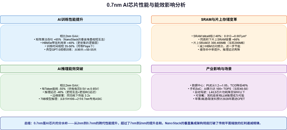
IBM’s published 0.7nm chip technology specifications:
| Metric | Value | Notes |
|---|---|---|
| Process Node | 0.7nm (7 angstrom) | World’s first sub-1nm technology |
| Transistor Architecture | NanoStack CFET | 3D vertical stacking |
| Transistor Density | ~98.6 billion/cm² | 2.03x vs 2nm |
| Performance Gain | Up to +50% | At same power |
| Energy Efficiency Gain | Up to +70% | At same compute |
| SRAM Scaling | 40% area reduction | Biggest in a decade |
| Reliability | ±12mV Vth drift | 1000-hour HTOL test |
| Peak Temp Reduction | 18°C lower | vs 2nm planar |
IV. Impact on AI Computing Infrastructure
4.1 New Dimensions in AI Chip Design
def nanostack_ai_impact():
    """
    Quantify NanoStack's impact on AI chip architecture
    """

    # Transistor budget comparison
    chips = {
        '2nm (B200-class)': {
            'total_B': 208,
            'compute': 0.30, 'sram': 0.45,
            'interconnect': 0.15, 'io': 0.10,
        },
        '0.7nm AI Chip': {
            'total_B': 420,
            'compute': 0.35, 'sram': 0.38,
            'interconnect': 0.17, 'io': 0.10,
        }
    }

    print("=" * 65)
    print("Transistor Budget: 2nm vs 0.7nm AI Chip")
    print("=" * 65)

    for name, b in chips.items():
        t = b['total_B']
        print(f"\n{name}:")
        print(f"  Total: {t}B ({t*10:.0f} billion)")
        for k, v in b.items():
            if k != 'total_B':
                print(f"  {k}: {v*100:.0f}% = {t*v:.1f}B transistors")

    # Inference performance simulation
    perf_boost = 1.50
    sram_boost = 1.40
    combined = perf_boost * sram_boost

    print(f"\nInference Performance Boost: {combined:.1f}x")
    models = [("GPT-5.6 1.8T", 1800, 1.0),
              ("LLaMA-4 405B", 405, 0.22),
              ("DeepSeek V4", 1000, 0.55)]

    print(f"\n{'Model':<22} {'2nm tok/s':<15} {'0.7nm tok/s':<15}")
    for name, _, tps in models:
        print(f"{name:<22} {tps:<15.1f} {tps*combined:<15.1f}")

    # Energy analysis
    p2nm, eff = 700, 0.70
    p07 = p2nm * (1 - eff)
    print(f"\nEnergy Efficiency:")
    print(f"  2nm power: {p2nm}W")
    print(f"  0.7nm power: {p07:.0f}W")
    print(f"  10K server cluster annual savings: {10000*(p2nm-p07)*8760/1e6:,.0f} MWh")

nanostack_ai_impact()
4.2 AI Chip Competitive Landscape Implications
NanoStack’s production timeline is estimated at 5 years (~2031). While this seems distant, the strategic implications are already unfolding:
For NVIDIA: Currently dependent on TSMC’s advanced nodes. NanoStack offers a path beyond traditional planar scaling. Future GPU architectures (Rubin Ultra beyond) could benefit from 3D stacking.
For IBM’s Strategy: Having exited manufacturing, IBM operates in an “architecture + R&D + licensing” model. NanoStack has already been licensed to Samsung and Japan’s Rapidus, meaning the technology will penetrate the AI chip supply chain through foundry partners.
For TSMC/Intel: TSMC’s 1.4nm roadmap and NanoStack’s 0.7nm are a full generation apart. If IBM’s licensing partners match the production timeline, the foundry market landscape could be reshaped.
Summary: IBM’s 0.7nm NanoStack technology is a genuine milestone—not incremental improvement, but a fundamental restructuring of 50 years of chip scaling logic. From planar to 3D, from nanometers to angstroms, NanoStack proves that chip performance improvement is not over. For the AI industry, this means the compute growth curve over the next decade will be steeper than anticipated.
References: IBM official press release, VLSI 2026 symposium papers, IT之家, Fast Technology, Sohu Tech, Pacific Tech